PCB- A Printed Circuit Board is the backbone of every electronic device. Today, we are surrounded by digital devices, and people use them without even understanding how it works. Various industries have been widely using PCB design services to develop a diversified range of electronic devices to ease our lives.
For example, the most important thing that we use daily in our lives is electricity. The modern lights have knocked down the incandescent lights with the help of a metal core PCB board that gives less heat. Many manufacturers use aluminium PCBs for efficient thermal transfer. The new technology signifies that if LEDs demand increases, PCBs will likely continue to play an important role in the electrical industry.
Any industry that needs electronics will require circuit board design services, and design the PCB layout effectively for the circuit boards to perform reliably. Have you ever wondered what a PCB is and how PCB designers customize the layout?
There must be multiple other queries running in your mind right now. Stick to the article to gain in-depth knowledge about PCB design.
What is PCB?

Everyone would have noticed a green board in every electronic device; yes, that’s precisely what is called a PCB—a well-designed and manufactured board with electrical components that are directly assembled to form a series of circuits. Manufacturing the bare green board is not possible without a PCB design consultant. It is a flat, rigid material with geometric patterns like circles, squares, rectangles and thin structures on one side.. Adding more layers makes the PCB more compact and easier to design.
By and large, PCB board design services can be a crucial task. However, the key to developing the apt layout is to create a schematic of the project. According to the research, the world market of bare PCBs is estimated to reach $79 billion by 2024.
To move further, there are many components, processes, and materials used in designing and manufacturing a PCB board. Before digging into each, let us understand the applications of PCB.
Applications of PCB in the Modern Society

Like the above image depicts, PCB is used in almost every industry that is continuously evolving. From kitchen appliances to smart gadgets, PCB is the heart of every electronic device today. As and when the electronic industry wants to launch a new device, a PCB design is necessary. With a plethora of functions, PCB works as a prototype for multiple sectors like below.
Smartphones and laptops have become a part of our life. The smart and sleek design we use needs high-volume PCBs for smooth functionality. The custom PCB cost is low per unit, keeping the overall process cost relatively feasible.
These days cars are upgrading with new technology and relying on electronic components. With the revolution of technologies incorporated in automobiles, high-frequency PCBs have increased, offering an improved driving experience to the customers. Control systems, navigation devices, media controls are some of the typical applications that function with the help of a PCB.
“With increasing concern of global emissions and fuel consumption from vehicles, the government has taken preventive measures of manufacturing Hybrid electric vehicles (HEV) and Battery electric vehicles (BEV) that will relatively; boost the automotive PCBs market growth.”
The growing demand for HEV and BEV vehicles is anticipated to register a CAGR of about 6% by 2025.
We are so used to handling our electrical devices carefully, so why not safeguard our lives too? With the help of PCB applications, security devices like burglar alarms, fire alarms, motion sensors, high-tech door locks, etc., are designed by electronic design and manufacturing companies for our safety.
There are multiple other industries that use PCBs for their products, but I believe these above-mentioned industries have the highest need for PCB design services. PCB solutions are needed across the globe. To understand the process involved in PCB design and layout services, continue reading further.
All the above applications if connected to the internet offers automation services to multiple industries. Learn how these wireless embedded devices help in different industries.
What is the PCB Design Services Process?
If you are planning to launch a product, you need to understand how a PCB works and what’s the process of designing a PCB. We have gathered the required process essential to design an effective PCB to get hardware product certification approval.
Step 1: Create a schematic
Creating a schematic for the project is all about drawing a blueprint of the new device. It should consist of the components of the design, how they are connected, and the relationship between the different components in one schematic.
Each schematic is created in the CAD system to design the PCB, representing the accurate pins that can be calculated eventually for the bills of materials.
Step 2: Create PCB layout with a schematic diagram
Creating a schematic may be easy, but converting the schematic to a board layout is easier. The right PCB layout designer will work on platforms such as Allegro, Altium, and Orcad to show how exactly your board will operate according to the position of the components.
A schematic capture tool, as mentioned above, can help to import the components in the PCB layout. A schematic design needs the shape, dimension, and layer to stack up initially, but if you are not sure of it, then fret not; that can be changed later. Once the schematic is created, the role of PCB engineering comes into the picture where they can initiate constructing PCB by analysing materials and recognizing the functionality of the device.
Step 3: PCB stackup
The growing demand for sleek and intelligent electronic products requires accurate multiple layers of PCB. Stack up has become popular to prevent complexities. If you are new to the PCB design process, the modern PCB design starts with an FR4 material, a two layer to sixteen or more layer board using a stack up a library that can help you understand different laminates and unique materials.
Step 4: Rules and requirements
The number of PCB rules is infinite, a PCB designer need not use all of them in the design layout. They can select the rules according to the device that needs to be manufactured. This step essentially involves the IPC standards for Component Footprint and PCB Fabrications which are the standardized criteria for PCB and electronic device manufacturing.
Tip: To get the best PCB design for your device, find a PCB design company that has the knowledge and is familiar with the IPC standards.
Step 5: Components Placement
A few software mentioned will help in placing the components that were created in the PCB schematic design. There may be a dispute to finalize which components can be placed near each other as a few might create electrical sound in the circuit. The components are usually placed in the following order:
Step 6: Vias and Drill holes (PTH and NPTH)
The bottleneck of PCB manufacturing is the drilling process. It is the foundation for the connectivity and the vias between multiple layers. The size of these via drill holes should typically be 0.25mm in diameter, and the mounting of these holes can be double-sided.
Step 7: Routing (Route the traces)
After each component is in place, the next step is routing. These are traces that become the metal connections in and on the circuit board while fabricating. Ensure that you use good routing guidelines with the help of the software, and to simplify the process, use color-coding and highlight nets.
Step 8: Silk Screen and Marking
Once the circuit board layout is ready with all the above processes, it is time to add labels and identifiers to the board. It is advisable to use reference identifiers for easy assistance while assembling. If there is any confusion, the designer can contact the device manufacturer for any specification on readable fonts for the logo and images.
It’s now time to hand over the file that contains the printed layout or a circuit board for manufacturing.
What are the materials used for manufacturing?
FR4 is used for manufacturing a PCB. FR4 is a glass fiber epoxy laminate for the multi-layer PCB design process. PCB boards that are made from FR4 are solid and water-resistant. It also gives good connectivity with minimal interference. FR4 material can work for several MHz to GHz frequencies. For High RF and Microwave frequencies many manufacturers prefer Roger PCB material as well. Based on the application and required temperature grade we need to select the right material.
Now that you are aware of how a PCB is designed, let us brief you about the different types of PCB design layout services available in the market.
Note that, the process to design a PCB remains same to any type of PCB service you use.
Types of PCB Services
PCBs are classified into multiple types based on the industry requirements, processes, product design specifications. More complex designs pave the way to different types of PCB service boards. Also the PCB design services cost will depend on which type of layer is used.
Before you pick up a PCB, consider a few features like space required, stress handling, and the product’s mechanical and electrical stability.
Let us study in detail the types of PCB layout services.
1. Single Sided PCBs
Single-sided conductive copper layer laminated above substrate. It is the start point for any PCB layout services technology and still plays an important role in any electrical product in the industry.
The electrical components are placed on one side and the etched circuit is visible on the other side of the board. These types of boards take up a lot of space as they are only conductive and cannot overlap. Single-layer is cheaper than any other type of PCB and an ideal choice for low density designs.
Advantage of Single Sided PCBs
2. Double Sided PCBs
A thin layer of conducting material is added on both sides of the double layer PCB. Holes in the circuit board allow the components to connect with each other. Through hole technology installing lead components becomes easy with soldered pads on both the sides.
Surface mount technology entails precise placement of the components of the PCB layout design. Double sided PCB is used for multiple applications like power monitoring, HVAC application, UPS systems, lighting systems, car dashboards, vending machines, etc.
Advantage of Double Sided Custom PCBs
3. Multilayer Sided PCBs
Multilayer PCB has more than two copper layers, so any application that is more complex will need at least three conductive layers. There are multiple double sided sheets divided into several layers.
All of these sheets and components are soldered and laminated in high temperature to ensure there are no gaps to prevent the instability of the final PCB. A few examples of multilayer PCBs are X-ray equipment, GPS technology, weather analytics devices, etc.
Advantage of Multilayer PCB Design & Layout Services
4. Rigid PCBs
As the name suggests, rigid PCBs are the ones that are not flexible or cannot be folded. The substrate is very rigid and holds the strength of the board components. There are multiple layers that include substrate, copper, solder mask, silk screen, that are combined together with heat to stay strong and rigid.
Rigid PCBs are used in computers, laptops, mobile phones, tablets, CAT scans, MRI systems, temperature sensors, etc.
Advantage of Rigid PCB Design Solutions
5. Flex PCBs
Recently, PCB design companies have adopted a new type of PCB designing that is Flex PCBs. Flex PCB is just the opposite of Rigid PCB, a flexible substrate with many printed circuits. Flexible PCB is made of polyether, ether and ketone, a transparent conductive polyester film using the same components as rigid printed circuit boards.
There are multiple names to this custom PCB design service like- Flex circuit boards, flex PCBs, flex circuits, and versatile printed circuits. Some of the applications that use flex PCBs are automotive industry, cellular telephones, complex electronics, LCD fabrication, etc.
Advantage of Flex Printed Circuit Board Design Services
6. Rigid-Flex PCBs
A flexi-rigid PCB is a hybrid PCB that combines both rigid and flex printed circuits. This results in a board that is flexible and typically shaped to curve and also stays rigid during the manufacturing process.
The flexible portion is typically used for interconnections with the rigid boards allowing conductor lines to take up less room. These boards are a little complicated to design as they are designed in 3D technology allowing the board to fold and twist as needed. Such boards are typically used in industries like medical, aerospace, and consumer fields.
Advantage of Rigid- Flex PCB Layout and Design Services
Check Out Our IoT Case Studies
Tips for the Best PCB Board Design
As we all know, our lives revolve around PCBs in the form of electronic devices, home appliances, smart gadgets, etc. we should be aware of how important a layout must be for the successful functioning of the device.
Below are a few tips that can help a novice printed circuit board designer to create the best layout.
The placement of each component is an art, and fine-tuning is deliberately required for effective performance. The process of placing each component is challenging and so, it is suggested to keep the guidelines in mind while designing the PCB layout.
Understanding the space between each component is crucial. The more components on the board, the more functionalities it would support on one device. It becomes challenging for the designer to keep appropriate spaces between the components for wire routing, and preventing the heat that can build up on the board.
With the components placed correctly and with the right amount of space, it’s time to route the power and signal traces to have an accessible path of travel. If your board forces for a horizontal trace, then route traces vertically on the opposite side exactly like the below image.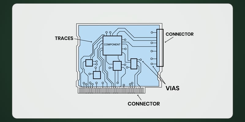
Combating the heat is always an issue in PCB. There are multiple ways to solve the heating issues, like distributing enough space between each component instead of clustering them in one layer and location. Another way is to add extra copper on the surface mount components. Also, we need to distribute the load across the PCB for better heat management.
-
Test Points and its location
This can help solve many designing issues while testing. The placement of test points should be accurate and accessible. If the test points are not accessible, the testing will be difficult. Efficient test points accessibility can solve all the testing issues.

Get updates of the latest tech news
Register with your email ID to get the first bite of the most trending news.
Are You Designing a New Product and Need a PCB Design Services?
We have skilled designers with years of experience in hardware engineering services who can provide you with custom PCB designing. Excellent Webworld has the best team of embedded software engineers to hire who can work on your project and deliver high-quality design. Our experts use different technologies like Rigid (2 layer to 12 layer), HDI (Blind-burried vias), Flex- Flex rigid for various applications like consumer electronics, IoT, RF product, Medical and Automotive. Along with these our team works on Altium and Cadence Allegro software to design your PCB and ensure guaranteed solutions that you can be proud of.
Summing up: Printed Circuit Board Design
Did you like reading the post?
We hope that the above information has given you everything that you were searching for. The PCB design services are highly customizable that enables it to produce complex and simple circuit functions. By following the process with a well-designed stack-up can result in an effective printed circuit board with multiple layers.
After all the factors mentioned above are taken into consideration, the manufacturing process starts. After the PCB is ready, product engineering services can help in testing the final product to ensure that the new device is ready to launch in the market. Reach out to us if you need more information on the circuit board design services, its cost and certifications.